How To Bypass China's Ban On Gallium Exports
In July 2023, China announced export controls on gallium, a critical component in the production of gallium arsenide (GaAs) wafers used in semiconductors, optoelectronics, and other high-tech applications. Given that China accounted for approximately 90% of global gallium production in 2022, these restrictions have significantly impacted the GaAs wafer market. USITCYole Group
The immediate effect was a sharp decline in China's gallium exports. For instance, in October 2023, China exported only 227 kg of gallium, a steep drop from the 6,876 kg exported in July 2023. This reduction led to supply constraints and price volatility in the global market. European gallium prices, for example, remained stable despite increased December exports from China, indicating persistent supply tightness. USITCFastmarkets
Manufacturers of GaAs wafers, such as AXT (USA), Freiberger (Germany), and Sumitomo Electric (Japan), have faced challenges due to these export controls. AXT, which manufactures all its products in China and partially owns Chinese raw material companies producing high-purity gallium, has been particularly affected. The company has applied for export licenses to continue supplying GaAs and germanium substrates. USITC+4Yole Group+4DIGITIMES Asia+4
In response to the supply constraints, there has been an increased focus on recycling gallium from scrap materials and seeking alternative sources outside China. However, establishing new production facilities or ramping up existing ones is a time-consuming process, leaving the GaAs wafer market vulnerable to ongoing disruptions. Financial Times
Overall, China's export controls on gallium have underscored the global semiconductor industry's reliance on Chinese supplies, prompting companies and governments to explore strategies for diversifying their sources of critical materials.Reuters+4Yole Group+4PIIE+4
Send us your specs/qty today for an immediate GaAs quote!
What Are Gallium Arsenide Wafers?
Gallium arsenide (GaAs) wafers are semiconductor materials made from a compound of gallium and arsenic. These wafers are prized for their high electron mobility, direct bandgap, and excellent thermal stability, making them ideal for advanced electronics and optoelectronics.
Applications of GaAs Wafers
- High-Frequency Electronics: RF amplifiers, microwave circuits, and millimeter-wave devices.

- Optoelectronics: LEDs, laser diodes, and photodetectors.
- Solar Cells: High-efficiency solar panels for space and terrestrial applications.
- Aerospace and Defense: Radar systems, satellite communication, and avionics.
- 5G and Telecommunications: Transceivers, antennas, and network components for 5G systems.
- Medical Devices: Infrared sensors and imaging equipment.
Advantages of GaAs Wafers
- Speed and Performance: Higher electron mobility enables faster devices.
- Optical Efficiency: Direct bandgap enhances light emission and absorption.
- Durability: Performs well under high temperatures and radiation.
- Low Noise: Produces less electronic noise in high-frequency applications.
What Does A Gallium Arsenide Wafer Look Like?
-
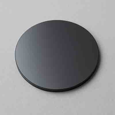
Color: GaAs wafers generally appear dark gray to almost black, often with a slight mirror-like sheen. They can also exhibit purple or bluish reflections under certain lighting because of their crystalline and polished surface.
-
Surface Finish: If the wafer is epiready or polished, it will be highly reflective. If it's semi-polished or etched, it may appear more matte or slightly hazy.
-
Backside: Often lapped (matte) and may look slightly different in color or texture compared to the shiny front.